
Products & Services
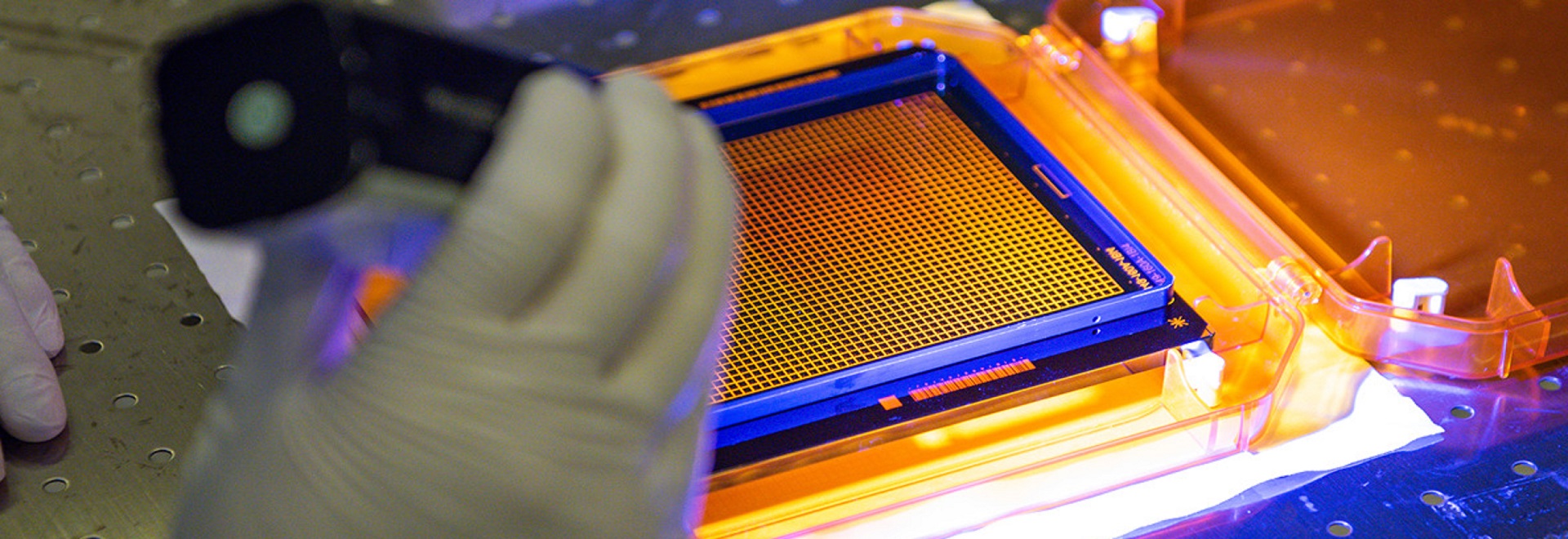
Photomask Production Process
Photomask Production Process
-
01CAM (Graphic Data Processing)Using computer software to convert product graphic files into formats recognizable by lithography systems. Also involves design, layout, and special compensations (e.g., DCM, OPC) on the original graphics/files, providing compensation and optimization for the product patterns and subsequent processes.
-
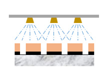
02Photoresist CoatingApplying a specific thickness and uniformity of photoresist onto a substrate already deposited with a chrome film. Baking solidifies the photoresist, enabling photochemical reactions under specific wavelength light, leading to the desired chrome pattern after subsequent development, etching, etc.
-
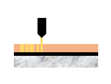
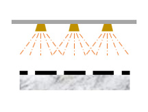
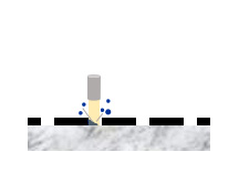
03Laser LithographyConverting design pattern data into control data for a laser direct writing system. A computer-controlled high-precision laser beam scans and writes the design pattern directly onto the photoresist-coated mask substrate according to the design file.
-
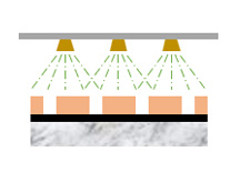
04DevelopmentUsing a chemical solution (developer) to interact with the photoresist, removing the exposed areas while leaving the unexposed areas intact, resulting in a photoresist pattern matching the design.
-
05EtchingAfter development, using a chemical solution (etchant) to react with and remove the chrome film not protected by photoresist. The chrome protected by photoresist remains.
-
06StrippingAfter etching, using a chemical solution to react with and completely remove any remaining photoresist from the mask, finally yielding the chrome pattern consistent with the design.
-
07CleaningUsing chemical solutions and pure water to clean the photomask, producing a product with surface cleanliness meeting specifications.
-
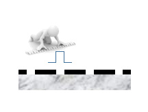
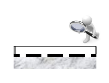
08Macro InspectionUsing light sources of different wavelengths and intensities to perform macro (visual) inspection of the mask surface to identify defects like Defect, Mura, Particle, etc.
-
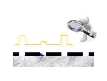
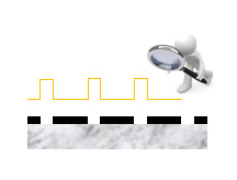
09Automatic Optical Inspection (AOI)Using a specific wavelength and intensity light source to capture the pattern of the product under test. A sensor (camera) acquires the illuminated image of the inspection pattern and digitizes it. Corresponding logic and software algorithms are then used for comparison, analysis, and judgment to check for surface defects like Line Open, Short, Intrusion, Pattern Missing, etc.
-
10Precision Measurement & CalibrationUsing high-precision measurement equipment to measure the Critical Dimension (CD) accuracy/uniformity, Total Pitch (TP) accuracy, Registration accuracy, etc., of the mask pattern, confirming if product precision meets specifications. Measurement results and related algorithms are also used to calibrate and compensate the mask and equipment platform to meet product requirements.
-
11Defect Processing/RepairFor defects like line breaks, intrusions, and pattern missing, Laser-Induced Chemical Vapor Deposition (LCVD) is used to deposit a thin film on the mask substrate for repair. For defects like chrome residues and shorts, lasers with specific energy are used for ablation/cutting.
-
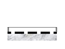
12Pellicle MountingA pellicle, made of polyester material, is mounted on the mask surface to protect it from contamination by dust, dirt, particles, etc.
-
Data Processing & Confirmation -
Direct Write Lithography -
Development -
Etching -
Stripping / Cleaning -
Dimensional Measurement (CD / Registration) -
Defect Inspection -
Defect Repair -
STARlight Inspection -
Pellicle Mounting -
Final Inspection -

Packaging & Shipping.